
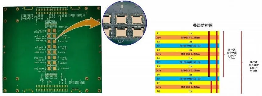
77 GHz radar high-frequency board
- Layers
- 18
- Materials
- TSM-DS3 + FR28 prepreg + S1000-2M, hybrid lamination
- Finish
- Immersion gold (ENIG)
- Special process
- Pure PTFE blind/buried-via impedance board, 5 back-drill groups
Complex interconnects, controlled impedance and specialty laminates for RF, high-speed and high-density designs, confirmed through engineering review for each project.
Advanced structures depend on the full design: stack-up, materials, via strategy and test method. We review these together and confirm feasibility before quotation.
Microvia and fine-line structures for dense BGA breakout and compact products.
Vias that connect only the layers that need them, freeing routing space in multilayer boards.
Removal of unused via stubs to reduce reflections on fast signals.
Trace geometry and dielectric choices matched to your impedance targets.
Multiple lamination cycles for complex via structures and hybrid constructions.
Complex stack-ups for communication, computing and test equipment.
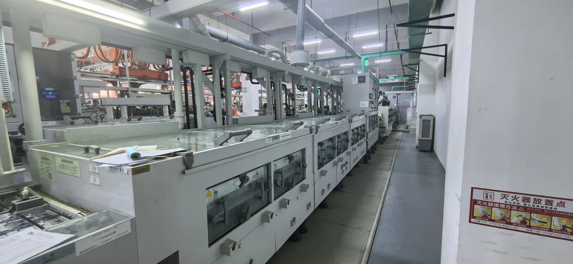
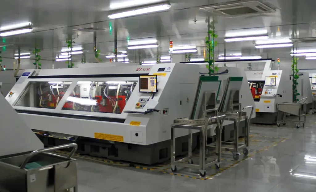
Board constructions from the ShinePCB company presentation — not customer references.
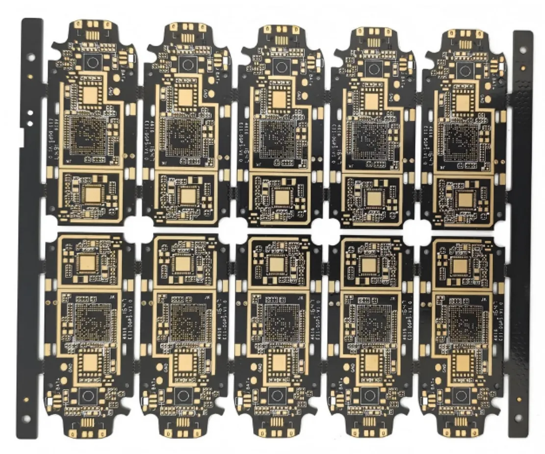
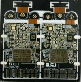
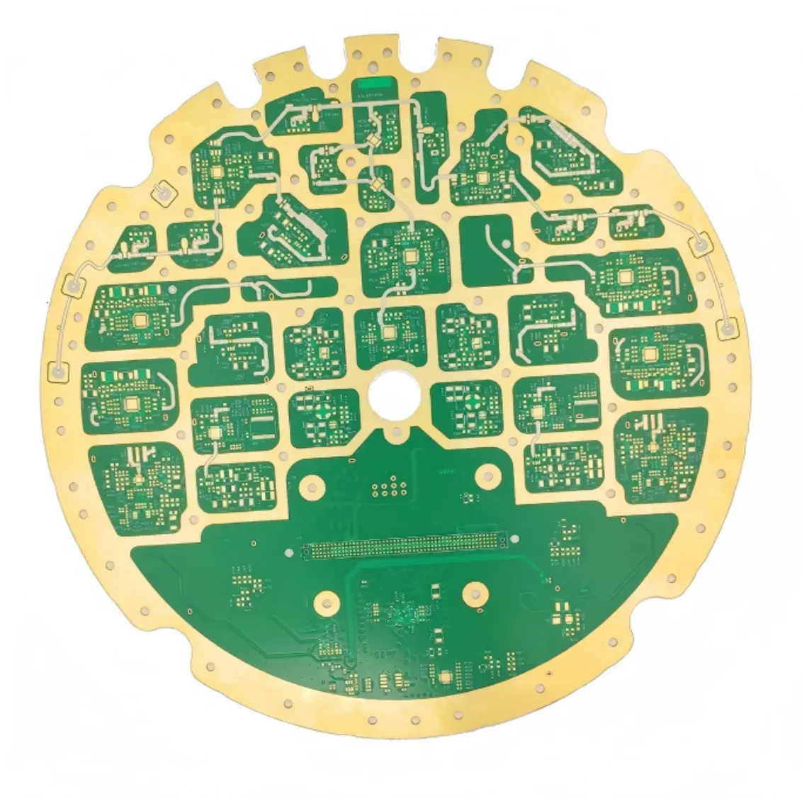
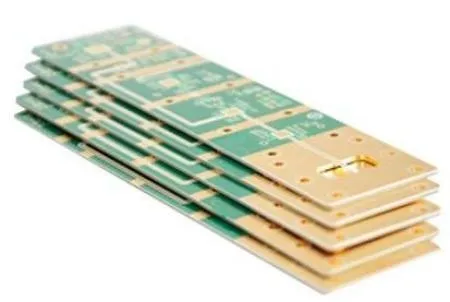
Builds from the ShinePCB company presentation. They illustrate process scope and are not customer references.
Material choice affects loss, stability, thermal performance and cost. Supplier datasheet values are material data, not fabrication guarantees; we confirm options and availability for each project.
Rogers laminates for RF and microwave circuits.
Isola laminates for high-speed digital and low-loss designs.
PTFE-based materials for demanding RF applications.
FR-4 with a higher glass-transition temperature for designs exposed to heat.
Share the details you have. Engineering reviews your requirements and raises questions before quotation.
Hybrid stack-ups are reviewed per project. We confirm compatibility and processing before quotation.
Impedance targets are reviewed with your stack-up and geometry, and the test method is agreed in the quotation. We do not assume a performance value without project review.
Every order follows the same controlled sequence. Prototype and production requirements are reviewed separately.
Gerber or ODB++, drill data, drawing and quantities are checked for completeness.
Open points on manufacturability, materials or special processes are sent before quotation.
Construction, laminate and finish are confirmed with you and written into the order.
The order is released to the facility whose process and qualification fit the requirements.
Inspection and electrical test follow the methods agreed for your order.
Boards are packed and shipped under the confirmed delivery terms.